- This topic is empty.
-
AuthorPosts
-
November 16, 2026 at 2:18 pm #114902
For SSD manufacturers, moving from a validated prototype to stable mass production can be more challenging than assembling the first working board. A design that performs correctly in a limited engineering build may encounter component shortages, soldering defects, signal-integrity problems, inconsistent test results, or yield variation when production volume increases. A qualified SSD board assembly supplier helps address these risks by connecting PCB fabrication, component procurement, assembly engineering, inspection, and functional validation within a controlled manufacturing process.
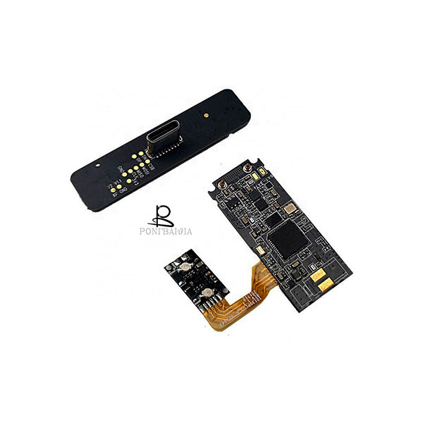
Production yield is influenced by the interaction between product design and manufacturing capability. Fine-pitch packages, dense routing, complex stack-ups, small passive components, and high-speed interfaces can all introduce constraints that should be identified before volume production begins. A structured engineering review is therefore more effective than relying on final inspection alone to identify defects after assembly.
Design for Manufacturability Before Production
Design for Manufacturability (DFM) evaluates whether a PCB design can be fabricated and assembled consistently using the intended manufacturing processes. For SSD boards, DFM should cover component spacing, pad geometry, solder-mask design, via placement, panelization, assembly access, and the relationship between high-speed routing and manufacturing constraints.
Component spacing is particularly important around fine-pitch controller and memory packages. Insufficient clearance can make solder-paste printing and inspection more difficult, increasing the risk of bridging or reducing the ability to rework defective joints. Pad dimensions and solder-mask openings should be reviewed against the component package requirements and the selected assembly process.
PCB fabrication constraints must also be considered early. Layer count, minimum trace and spacing, via dimensions, copper thickness, and stack-up affect manufacturability and cost. For high-speed SSD designs, any proposed change must preserve the electrical requirements of the interface. A trace-width adjustment that improves fabrication yield but changes controlled impedance cannot be accepted without appropriate engineering review.
Panelization is another practical consideration. A suitable panel design supports stable handling during printing, placement, reflow, and depanelization. Fiducial placement, tooling features, board support, and breakaway structures should be coordinated with the assembly equipment and the PCB outline. Poor panel design can cause handling difficulties even when the individual board layout is electrically sound.
The most useful DFM feedback is specific and actionable. Rather than simply marking a layout as difficult to manufacture, the supplier should identify the affected feature, explain the process risk, and propose a technically acceptable alternative. Design changes should be reviewed against electrical performance, mechanical fit, cost, and reliability before the production files are released.
Component Availability and Revision Management
Component sourcing can become a major production risk when an SSD design relies on controllers, NAND flash packages, or other components with limited availability. A board may be technically ready for production but unable to enter assembly because one critical component is delayed or discontinued.
A BOM review should identify long-lead-time parts, supplier concentration, lifecycle status, approved alternates, and any components requiring customer authorization before substitution. This is particularly important for memory and controller devices because nominally similar parts may differ in supported protocols, firmware requirements, package pinout, timing, or power behavior.
Revision management must cover both hardware and production data. The approved BOM, PCB fabrication files, assembly drawings, pick-and-place data, firmware version where relevant, and test instructions should correspond to the same product revision. Mixing data from different revisions can lead to assembly errors or test failures that are difficult to diagnose.
A controlled engineering-change process should define who can authorize a change, what documentation must be updated, and how existing inventory will be handled. If a component is substituted, the change may require more than a visual or dimensional check. Electrical compatibility, firmware interaction, thermal characteristics, and functional performance may need to be verified before release.
An integrated SSD board assembly supplier can coordinate PCB fabrication and component procurement more efficiently, but supply-chain visibility remains essential. Customers should be able to review the status of critical materials and understand the implications of any proposed change to the approved configuration.
SMT Process Control and Defect Prevention
Surface-mount assembly is a major determinant of board quality. The process includes solder-paste printing, component placement, reflow soldering, and post-assembly inspection. Each stage introduces potential failure modes, and defects from early stages can propagate into later operations.
Solder-paste printing requires appropriate stencil design, paste handling, alignment, and process control. Excessive or insufficient paste volume can lead to bridging, opens, or weak solder joints. For dense SSD layouts, aperture design and printing consistency should be evaluated in relation to component pitch and pad geometry.
Component placement should be controlled through verified placement programs, correct package data, feeder setup, and orientation checks. Incorrect rotation, offset placement, or a mismatch between the component library and the actual package can create defects that are not always obvious during manual review. Program verification before a production run helps reduce avoidable errors.
Reflow soldering must follow a profile appropriate to the solder paste, component specifications, PCB construction, and thermal mass. Excessive heating can stress components or the PCB, while insufficient heating may produce incomplete soldering. The profile should be established and verified for the actual assembly rather than copied without assessment from an unrelated product.
Defect prevention is more efficient when process data is reviewed together with inspection results. If solder bridges occur repeatedly in a particular area, the cause may involve stencil aperture design, paste volume, component spacing, or printing conditions. A corrective action that addresses the source of the problem can improve yield more effectively than increasing downstream inspection alone.
Inspection Strategy: AOI, X-Ray, and Electrical Testing
An effective inspection plan uses methods that match the likely defect types. Automated Optical Inspection can identify many visible defects, including missing or misaligned components, incorrect orientation, solder bridges, and certain solder-joint anomalies. It is valuable for consistent inspection at production speed, but its coverage is limited by visibility and the characteristics of the package.
For area-array packages or components with hidden solder connections, X-ray inspection may be appropriate. It can reveal certain hidden-joint defects that optical inspection cannot see directly. The inspection criteria should reflect the package design and applicable acceptance standards; an X-ray image alone does not establish overall electrical or functional performance.
Flying probe testing is useful for selected electrical checks, particularly during prototypes and low-volume production where dedicated fixtures may not be economical. ICT can provide repeatable electrical testing when the board design and access points support the required coverage. These methods detect different categories of faults, so their roles should be defined rather than treating them as interchangeable.
Functional testing verifies the behavior of the assembled SSD at the device level. Depending on the product, the test sequence may include power-up, device identification, interface communication, storage access, read/write operations, and selected performance or thermal checks. The test environment should be controlled because host configuration, firmware, workload, and drive condition can influence the results.
For example, a performance test that does not define transfer size, queue depth, workload, and test duration may produce inconsistent results across production stations. Clear test parameters improve repeatability and make failures easier to reproduce. Test limits should be derived from the product specification and validation results, not chosen solely to maximize apparent pass rates.
Yield Analysis and Root-Cause Investigation
First-pass yield provides a useful view of how many units pass the defined manufacturing and test stages without rework. However, the figure is meaningful only when the measurement scope and denominator are clearly defined. A yield report should distinguish initial pass rate, rework recovery, final acceptance, and scrap where these categories are tracked.
Defect Pareto analysis can help prioritize improvement work by identifying the most frequent or costly failure categories. For SSD board assembly, issues may arise from soldering, component placement, PCB fabrication, component defects, configuration mismatches, or functional-test setup. The correct corrective action depends on the evidence, not on assuming that all failures originate in SMT.
Root-cause investigation should combine defect location, process records, inspection images, test logs, material lot information, and relevant design details. When necessary, failed units can be examined through component replacement, electrical measurement, microscopy, or other suitable analysis. The goal is to distinguish the actual failure mechanism from symptoms observed at final test.
After corrective action, the process should be monitored to confirm that the issue has been reduced without introducing new problems. Changes to stencil design, reflow profiles, PCB fabrication, component sourcing, or test software should be documented and verified. This creates a learning cycle that improves process stability over successive production runs.
Traceability and Reliability Requirements
Traceability becomes especially valuable when an SSD is used in industrial control, embedded computing, communication equipment, or other applications where failures can disrupt a larger system. A traceability system should connect finished units or production lots to relevant material batches, assembly records, inspection results, and functional-test data.
The level of traceability should match the customer’s quality requirements. Some projects may require lot-level records, while others may need unit-level serial-number tracking and test-result retention. These requirements should be agreed before production begins because they can influence labeling, software integration, data storage, and manufacturing workflow.
Reliability validation should also be distinguished from routine production testing. A functional test confirms that the product meets defined operating criteria at the time of testing. It does not automatically prove long-term endurance, environmental resistance, or lifetime performance. Where the application requires thermal cycling, vibration, power cycling, or other stress testing, those activities should be defined within the product validation plan.
For high-speed SSDs, thermal performance and signal integrity can also require system-level consideration. The PCB, controller, memory, power circuitry, enclosure, and host interface work together. A board that passes basic electrical checks may still need further validation under the intended workload or operating temperature.
Integrated Manufacturing Support From Rongbaijia Technology
Shenzhen Rongbaijia Technology Co., Ltd. provides PCB manufacturing and one-stop PCBA services, integrating design support, component sourcing, SMT assembly, through-hole soldering, and testing. The company reports capabilities in multilayer and HDI PCB production, impedance control, seven automated SMT lines, two wave-soldering machines, AOI, flying probe testing, and ICT/FCT services.
These capabilities can support an SSD manufacturing workflow that requires close coordination between board fabrication and assembly. Its DFM engineering support is relevant during early design review, while integrated sourcing and testing can reduce the number of separate suppliers involved in production. For a specific SSD project, however, the required layer stack-up, impedance tolerances, package inspection methods, test coverage, and traceability level should be confirmed against the actual design and product specification.
Conclusion
Reducing SSD manufacturing risk requires attention to the entire process, from design review and BOM control to SMT process stability, inspection, functional testing, and root-cause analysis. No single inspection method can eliminate every defect, and high nominal production capacity does not by itself guarantee consistent yield.
A qualified SSD board assembly supplier should combine engineering feedback with controlled manufacturing, suitable test coverage, traceable records, and disciplined change management. When these capabilities are established before mass production, manufacturers are better positioned to improve yield, shorten troubleshooting cycles, and maintain consistent product quality as demand scales.
http://www.rbjpcb.com
Shenzhen Rongbaijia Technology Co., Ltd. -
AuthorPosts

- You must be logged in to reply to this topic.