- This topic is empty.
-
AuthorPosts
-
January 3, 2025 at 5:31 pm #109547
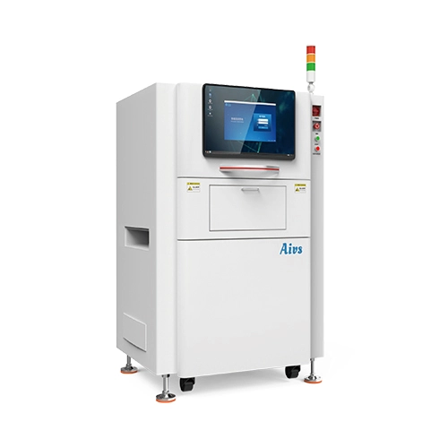
Any small defect or error can lead to product failure, reputation damage or even safety risks. This is where Automated Optical Inspection (AOI) comes into play. AOI has become a critical part of the assembly process, especially for industries that require precision and high quality. In this blog post, AlVS will share the working principle of AOI Auto Optical Inspection for sale and its importance in improving efficiency and quality in electronics manufacturing.
What is AOI Auto Optical Inspection?
AOI stands for Automatic Optical Inspection, and it is a non-destructive, automated process used to inspect the quality of soldering and components on a printed circuit board (PCB) during the manufacturing process. It involves the use of cameras and specialized software to visually inspect the components, ensuring that all parts are correctly placed and soldered. Any discrepancies—such as misplaced components, soldering defects, or shorts—are detected and flagged for correction.
AOI can be performed at various stages of PCB production, including after the solder paste application, during the placement of components, and after the soldering process.
Working Principle of AOI Auto Optical Inspection
The working of AOI systems can be broken down into several stages, each crucial to its ability to detect defects and ensure high-quality manufacturing. Let' s look at how AOI works step by step.
1. Pre-Inspection Setup:
Before an AOI system can perform its inspection, it requires some setup. This setup involves feeding the system with the required reference data, which usually comes from the design files of the PCB. These files might include Gerber files, Bill of Materials (BOM), or CAD data, which define the layout of the board, the position of components, and their respective characteristics.
This information is essential for the AOI system to know what a "correct" PCB should look like, so it can identify any deviations from the norm.
2. Image Acquisition:
The first physical step in the AOI process is capturing high-resolution images of the PCB. Specialized cameras, often high-definition digital or 3D cameras, are positioned above or around the board. These cameras are capable of capturing images from different angles to ensure complete coverage.
In some systems, multiple cameras may be used simultaneously to inspect different areas of the PCB, ensuring faster inspection times. The images are taken in real-time as the PCB passes through the inspection area, often on a conveyor belt.

3. Image Processing:
Once the images are captured, they are fed into powerful image processing software, which uses advanced algorithms to analyze the captured data. The software compares the images against the reference data to detect any discrepancies. The system checks for various types of defects, including:
– Missing or Misplaced Components: AOI can identify if a component is missing or incorrectly placed.
– Soldering Defects: These may include insufficient solder, excessive solder, or solder bridges.
– Component Orientation: In some cases, components need to be placed in a specific orientation. AOI ensures that all components are properly aligned.
– Surface Defects: AOI can also detect surface issues like scratches or stains on the PCB.
The system uses a combination of color analysis, shape recognition, and edge detection to find these errors. For example, a "good" solder joint will have specific characteristics, like a certain color and shape. If the system detects a deviation, it flags the area for further review.
4. Error Detection and Classification:
After processing the images and comparing them to the design files, the AOI system classifies any detected defects into categories, such as minor, major, or critical. The severity of the defect determines whether the board needs to be reworked or discarded.
If a defect is found, the system will highlight the location and nature of the defect, which is then reviewed by an operator or sent to an automated rework station. Some AOI systems can even integrate with other systems, like Automated X-ray Inspection (AXI), for more detailed inspection of hidden defects, such as those beneath components or within vias.
5. Reporting and Feedback:
After the inspection, the AOI system generates a detailed report that documents any defects found, along with their severity and location. This report can be analyzed by engineers to make decisions on whether a board can proceed in the production process or needs adjustments.
Many AOI systems are equipped with real-time feedback mechanisms that allow manufacturers to make on-the-spot corrections. This can involve adjusting the soldering process, recalibrating the pick-and-place machines, or simply correcting a placement error.
Benefits of AOI in Electronics Manufacturing
The implementation of AOI in electronics manufacturing offers several significant benefits:
– Improved Quality Control: AOI ensures that every PCB is inspected thoroughly, leading to higher product quality with fewer defects.
– Increased Efficiency: By automating the inspection process, AOI systems can perform much faster than manual inspection, improving overall production speed.
– Cost Reduction: Early detection of defects reduces the need for rework and scrap, ultimately lowering production costs.
– Consistent Results: AOI systems deliver consistent inspection results, eliminating human error and subjective judgment, which can vary from operator to operator.
– Traceability: AOI provides detailed records of the inspection process, which helps manufacturers track quality over time and improve their processes.
Conclusion
Automated Optical Inspection (AOI) has changed the way electronics manufacturers inspect PCBs. With its ability to quickly and accurately identify defects, AOI plays a vital role in ensuring the quality, efficiency, and cost-effectiveness of electronics production. As the demand for high-quality electronics continues to grow, AOI will only become more critical, offering manufacturers the tools they need to maintain competitive advantage and produce flawless products. Whether you're designing a consumer gadget, medical device, or automotive system, understanding how AOI works is essential for anyone involved in the manufacturing process.
-
AuthorPosts
- You must be logged in to reply to this topic.